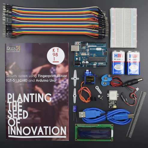
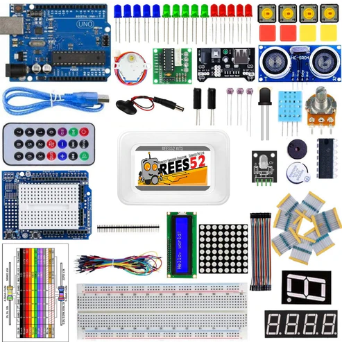
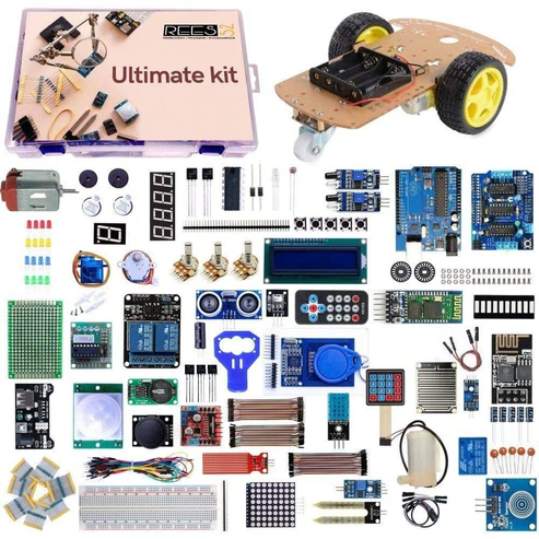
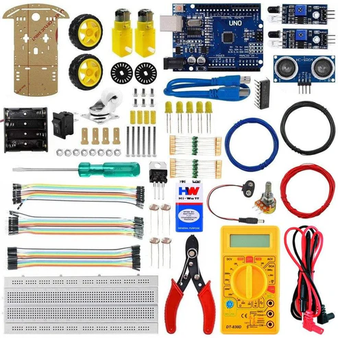
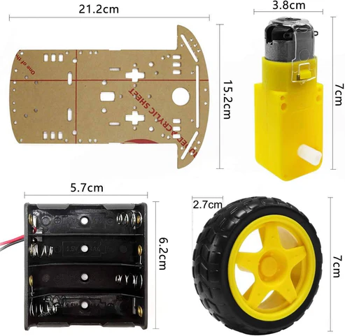
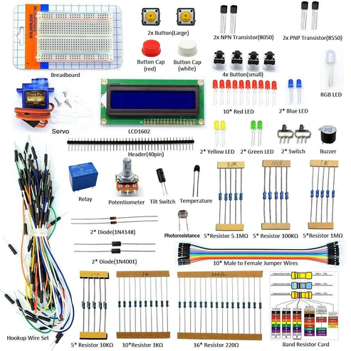
KIT INCLUDES:
The camera module is powered from a single +3.3V power supply. An external oscillator provide the clock source for camera module XCLK pin. With proper configuration to the camera internal registers via I2C bus, then the camera supply pixel clock (PCLK) and camera data back to the host with synchronize signal like HREF and VSYNC. The OV7670 camera module is a low cost 0.3 mega pixel CMOS color camera module, it can output 640×480 VGA resolution image at 30fps. The OV7670 camera module build in onboard LDO regulator only single 3.3V power needed and can be used in Arduino, STM32,Chipkit, ARM, DSP , FPGA and etc.
HARDWARE REQUIRED
SOFTWARE REQUIRED
Arduino IDE
Arduino IDE 1.8.5 (programmable platform for Arduino)
Click To Download:https://www.arduino.cc/en/Main/Software

Code
Click to see the code or copy the link.
https://drive.google.com/open?id=1jw0vFKKPVtBTvKHk42uYc0OuB1QG08xi
#include <stdint.h>
#include <avr/io.h>
#include <util/twi.h>
#include <util/delay.h>
#include <avr/pgmspace.h>
#define F_CPU 16000000UL
#define vga 0
#define qvga 1
#define qqvga 2
#define yuv422 0
#define rgb565 1
#define bayerRGB 2
#define camAddr_WR 0x42
#define camAddr_RD 0x43
/* Registers */
#define REG_GAIN 0x00 /* Gain lower 8 bits (rest in vref) */
#define REG_BLUE 0x01 /* blue gain */
#define REG_RED 0x02 /* red gain */
#define REG_VREF 0x03 /* Pieces of GAIN, VSTART, VSTOP */
#define REG_COM1 0x04 /* Control 1 */
#define COM1_CCIR656 0x40 /* CCIR656 enable */
#define REG_BAVE 0x05 /* U/B Average level */
#define REG_GbAVE 0x06 /* Y/Gb Average level */
#define REG_AECHH 0x07 /* AEC MS 5 bits */
#define REG_RAVE 0x08 /* V/R Average level */
#define REG_COM2 0x09 /* Control 2 */
#define COM2_SSLEEP 0x10 /* Soft sleep mode */
#define REG_PID 0x0a /* Product ID MSB */
#define REG_VER 0x0b /* Product ID LSB */
#define REG_COM3 0x0c /* Control 3 */
#define COM3_SWAP 0x40 /* Byte swap */
#define COM3_SCALEEN 0x08 /* Enable scaling */
#define COM3_DCWEN 0x04 /* Enable downsamp/crop/window */
#define REG_COM4 0x0d /* Control 4 */
#define REG_COM5 0x0e /* All “reserved” */
#define REG_COM6 0x0f /* Control 6 */
#define REG_AECH 0x10 /* More bits of AEC value */
#define REG_CLKRC 0x11 /* Clocl control */
#define CLK_EXT 0x40 /* Use external clock directly */
#define CLK_SCALE 0x3f /* Mask for internal clock scale */
#define REG_COM7 0x12 /* Control 7 */ //REG mean address.
#define COM7_RESET 0x80 /* Register reset */
#define COM7_FMT_MASK 0x38
#define COM7_FMT_VGA 0x00
#define COM7_FMT_CIF 0x20 /* CIF format */
#define COM7_FMT_QVGA 0x10 /* QVGA format */
#define COM7_FMT_QCIF 0x08 /* QCIF format */
#define COM7_RGB 0x04 /* bits 0 and 2 – RGB format */
#define COM7_YUV 0x00 /* YUV */
#define COM7_BAYER 0x01 /* Bayer format */
#define COM7_PBAYER 0x05 /* “Processed bayer” */
#define REG_COM8 0x13 /* Control 8 */
#define COM8_FASTAEC 0x80 /* Enable fast AGC/AEC */
#define COM8_AECSTEP 0x40 /* Unlimited AEC step size */
#define COM8_BFILT 0x20 /* Band filter enable */
#define COM8_AGC 0x04 /* Auto gain enable */
#define COM8_AWB 0x02 /* White balance enable */
#define COM8_AEC 0x01 /* Auto exposure enable */
#define REG_COM9 0x14 /* Control 9- gain ceiling */
#define REG_COM10 0x15 /* Control 10 */
#define COM10_HSYNC 0x40 /* HSYNC instead of HREF */
#define COM10_PCLK_HB 0x20 /* Suppress PCLK on horiz blank */
#define COM10_HREF_REV 0x08 /* Reverse HREF */
#define COM10_VS_LEAD 0x04 /* VSYNC on clock leading edge */
#define COM10_VS_NEG 0x02 /* VSYNC negative */
#define COM10_HS_NEG 0x01 /* HSYNC negative */
#define REG_HSTART 0x17 /* Horiz start high bits */
#define REG_HSTOP 0x18 /* Horiz stop high bits */
#define REG_VSTART 0x19 /* Vert start high bits */
#define REG_VSTOP 0x1a /* Vert stop high bits */
#define REG_PSHFT 0x1b /* Pixel delay after HREF */
#define REG_MIDH 0x1c /* Manuf. ID high */
#define REG_MIDL 0x1d /* Manuf. ID low */
#define REG_MVFP 0x1e /* Mirror / vflip */
#define MVFP_MIRROR 0x20 /* Mirror image */
#define MVFP_FLIP 0x10 /* Vertical flip */
#define REG_AEW 0x24 /* AGC upper limit */
#define REG_AEB 0x25 /* AGC lower limit */
#define REG_VPT 0x26 /* AGC/AEC fast mode op region */
#define REG_HSYST 0x30 /* HSYNC rising edge delay */
#define REG_HSYEN 0x31 /* HSYNC falling edge delay */
#define REG_HREF 0x32 /* HREF pieces */
#define REG_TSLB 0x3a /* lots of stuff */
#define TSLB_YLAST 0x04 /* UYVY or VYUY – see com13 */
#define REG_COM11 0x3b /* Control 11 */
#define COM11_NIGHT 0x80 /* NIght mode enable */
#define COM11_NMFR 0x60 /* Two bit NM frame rate */
#define COM11_HZAUTO 0x10 /* Auto detect 50/60 Hz */
#define COM11_50HZ 0x08 /* Manual 50Hz select */
#define COM11_EXP 0x02
#define REG_COM12 0x3c /* Control 12 */
#define COM12_HREF 0x80 /* HREF always */
#define REG_COM13 0x3d /* Control 13 */
#define COM13_GAMMA 0x80 /* Gamma enable */
#define COM13_UVSAT 0x40 /* UV saturation auto adjustment */
#define COM13_UVSWAP 0x01 /* V before U – w/TSLB */
#define REG_COM14 0x3e /* Control 14 */
#define COM14_DCWEN 0x10 /* DCW/PCLK-scale enable */
#define REG_EDGE 0x3f /* Edge enhancement factor */
#define REG_COM15 0x40 /* Control 15 */
#define COM15_R10F0 0x00 /* Data range 10 to F0 */
#define COM15_R01FE 0x80 /* 01 to FE */
#define COM15_R00FF 0xc0 /* 00 to FF */
#define COM15_RGB565 0x10 /* RGB565 output */
#define COM15_RGB555 0x30 /* RGB555 output */
#define REG_COM16 0x41 /* Control 16 */
#define COM16_AWBGAIN 0x08 /* AWB gain enable */
#define REG_COM17 0x42 /* Control 17 */
#define COM17_AECWIN 0xc0 /* AEC window – must match COM4 */
#define COM17_CBAR 0x08 /* DSP Color bar */
/*
* This matrix defines how the colors are generated, must be
* tweaked to adjust hue and saturation.
*
* Order: v-red, v-green, v-blue, u-red, u-green, u-blue
* They are nine-bit signed quantities, with the sign bit
* stored in0x58.Sign for v-red is bit 0, and up from there.
*/
#define REG_CMATRIX_BASE 0x4f
#define CMATRIX_LEN 6
#define REG_CMATRIX_SIGN 0x58
#define REG_BRIGHT 0x55 /* Brightness */
#define REG_CONTRAS 0x56 /* Contrast control */
#define REG_GFIX 0x69 /* Fix gain control */
#define REG_REG76 0x76 /* OV’s name */
#define R76_BLKPCOR 0x80 /* Black pixel correction enable */
#define R76_WHTPCOR 0x40 /* White pixel correction enable */
#define REG_RGB444 0x8c /* RGB 444 control */
#define R444_ENABLE 0x02 /* Turn on RGB444, overrides 5×5 */
#define R444_RGBX 0x01 /* Empty nibble at end */
#define REG_HAECC1 0x9f /* Hist AEC/AGC control 1 */
#define REG_HAECC2 0xa0 /* Hist AEC/AGC control 2 */
#define REG_BD50MAX 0xa5 /* 50hz banding step limit */
#define REG_HAECC3 0xa6 /* Hist AEC/AGC control 3 */
#define REG_HAECC4 0xa7 /* Hist AEC/AGC control 4 */
#define REG_HAECC5 0xa8 /* Hist AEC/AGC control 5 */
#define REG_HAECC6 0xa9 /* Hist AEC/AGC control 6 */
#define REG_HAECC7 0xaa /* Hist AEC/AGC control 7 */
#define REG_BD60MAX 0xab /* 60hz banding step limit */
#define REG_GAIN 0x00 /* Gain lower 8 bits (rest in vref) */
#define REG_BLUE 0x01 /* blue gain */
#define REG_RED 0x02 /* red gain */
#define REG_VREF 0x03 /* Pieces of GAIN, VSTART, VSTOP */
#define REG_COM1 0x04 /* Control 1 */
#define COM1_CCIR656 0x40 /* CCIR656 enable */
#define REG_BAVE 0x05 /* U/B Average level */
#define REG_GbAVE 0x06 /* Y/Gb Average level */
#define REG_AECHH 0x07 /* AEC MS 5 bits */
#define REG_RAVE 0x08 /* V/R Average level */
#define REG_COM2 0x09 /* Control 2 */
#define COM2_SSLEEP 0x10 /* Soft sleep mode */
#define REG_PID 0x0a /* Product ID MSB */
#define REG_VER 0x0b /* Product ID LSB */
#define REG_COM3 0x0c /* Control 3 */
#define COM3_SWAP 0x40 /* Byte swap */
#define COM3_SCALEEN 0x08 /* Enable scaling */
#define COM3_DCWEN 0x04 /* Enable downsamp/crop/window */
#define REG_COM4 0x0d /* Control 4 */
#define REG_COM5 0x0e /* All “reserved” */
#define REG_COM6 0x0f /* Control 6 */
#define REG_AECH 0x10 /* More bits of AEC value */
#define REG_CLKRC 0x11 /* Clocl control */
#define CLK_EXT 0x40 /* Use external clock directly */
#define CLK_SCALE 0x3f /* Mask for internal clock scale */
#define REG_COM7 0x12 /* Control 7 */
#define COM7_RESET 0x80 /* Register reset */
#define COM7_FMT_MASK 0x38
#define COM7_FMT_VGA 0x00
#define COM7_FMT_CIF 0x20 /* CIF format */
#define COM7_FMT_QVGA 0x10 /* QVGA format */
#define COM7_FMT_QCIF 0x08 /* QCIF format */
#define COM7_RGB 0x04 /* bits 0 and 2 – RGB format */
#define COM7_YUV 0x00 /* YUV */
#define COM7_BAYER 0x01 /* Bayer format */
#define COM7_PBAYER 0x05 /* “Processed bayer” */
#define REG_COM8 0x13 /* Control 8 */
#define COM8_FASTAEC 0x80 /* Enable fast AGC/AEC */
#define COM8_AECSTEP 0x40 /* Unlimited AEC step size */
#define COM8_BFILT 0x20 /* Band filter enable */
#define COM8_AGC 0x04 /* Auto gain enable */
#define COM8_AWB 0x02 /* White balance enable */
#define COM8_AEC 0x01 /* Auto exposure enable */
#define REG_COM9 0x14 /* Control 9- gain ceiling */
#define REG_COM10 0x15 /* Control 10 */
#define COM10_HSYNC 0x40 /* HSYNC instead of HREF */
#define COM10_PCLK_HB 0x20 /* Suppress PCLK on horiz blank */
#define COM10_HREF_REV 0x08 /* Reverse HREF */
#define COM10_VS_LEAD 0x04 /* VSYNC on clock leading edge */
#define COM10_VS_NEG 0x02 /* VSYNC negative */
#define COM10_HS_NEG 0x01 /* HSYNC negative */
#define REG_HSTART 0x17 /* Horiz start high bits */
#define REG_HSTOP 0x18 /* Horiz stop high bits */
#define REG_VSTART 0x19 /* Vert start high bits */
#define REG_VSTOP 0x1a /* Vert stop high bits */
#define REG_PSHFT 0x1b /* Pixel delay after HREF */
#define REG_MIDH 0x1c /* Manuf. ID high */
#define REG_MIDL 0x1d /* Manuf. ID low */
#define REG_MVFP 0x1e /* Mirror / vflip */
#define MVFP_MIRROR 0x20 /* Mirror image */
#define MVFP_FLIP 0x10 /* Vertical flip */
#define REG_AEW 0x24 /* AGC upper limit */
#define REG_AEB 0x25 /* AGC lower limit */
#define REG_VPT 0x26 /* AGC/AEC fast mode op region */
#define REG_HSYST 0x30 /* HSYNC rising edge delay */
#define REG_HSYEN 0x31 /* HSYNC falling edge delay */
#define REG_HREF 0x32 /* HREF pieces */
#define REG_TSLB 0x3a /* lots of stuff */
#define TSLB_YLAST 0x04 /* UYVY or VYUY – see com13 */
#define REG_COM11 0x3b /* Control 11 */
#define COM11_NIGHT 0x80 /* NIght mode enable */
#define COM11_NMFR 0x60 /* Two bit NM frame rate */
#define COM11_HZAUTO 0x10 /* Auto detect 50/60 Hz */
#define COM11_50HZ 0x08 /* Manual 50Hz select */
#define COM11_EXP 0x02
#define REG_COM12 0x3c /* Control 12 */
#define COM12_HREF 0x80 /* HREF always */
#define REG_COM13 0x3d /* Control 13 */
#define COM13_GAMMA 0x80 /* Gamma enable */
#define COM13_UVSAT 0x40 /* UV saturation auto adjustment */
#define COM13_UVSWAP 0x01 /* V before U – w/TSLB */
#define REG_COM14 0x3e /* Control 14 */
#define COM14_DCWEN 0x10 /* DCW/PCLK-scale enable */
#define REG_EDGE 0x3f /* Edge enhancement factor */
#define REG_COM15 0x40 /* Control 15 */
#define COM15_R10F0 0x00 /* Data range 10 to F0 */
#define COM15_R01FE 0x80 /* 01 to FE */
#define COM15_R00FF 0xc0 /* 00 to FF */
#define COM15_RGB565 0x10 /* RGB565 output */
#define COM15_RGB555 0x30 /* RGB555 output */
#define REG_COM16 0x41 /* Control 16 */
#define COM16_AWBGAIN 0x08 /* AWB gain enable */
#define REG_COM17 0x42 /* Control 17 */
#define COM17_AECWIN 0xc0 /* AEC window – must match COM4 */
#define COM17_CBAR 0x08 /* DSP Color bar */
#define CMATRIX_LEN 6
#define REG_BRIGHT 0x55 /* Brightness */
#define REG_REG76 0x76 /* OV’s name */
#define R76_BLKPCOR 0x80 /* Black pixel correction enable */
#define R76_WHTPCOR 0x40 /* White pixel correction enable */
#define REG_RGB444 0x8c /* RGB 444 control */
#define R444_ENABLE 0x02 /* Turn on RGB444, overrides 5×5 */
#define R444_RGBX 0x01 /* Empty nibble at end */
#define REG_HAECC1 0x9f /* Hist AEC/AGC control 1 */
#define REG_HAECC2 0xa0 /* Hist AEC/AGC control 2 */
#define REG_BD50MAX 0xa5 /* 50hz banding step limit */
#define REG_HAECC3 0xa6 /* Hist AEC/AGC control 3 */
#define REG_HAECC4 0xa7 /* Hist AEC/AGC control 4 */
#define REG_HAECC5 0xa8 /* Hist AEC/AGC control 5 */
#define REG_HAECC6 0xa9 /* Hist AEC/AGC control 6 */
#define REG_HAECC7 0xaa /* Hist AEC/AGC control 7 */
#define REG_BD60MAX 0xab /* 60hz banding step limit */
#define MTX1 0x4f /* Matrix Coefficient 1 */
#define MTX2 0x50 /* Matrix Coefficient 2 */
#define MTX3 0x51 /* Matrix Coefficient 3 */
#define MTX4 0x52 /* Matrix Coefficient 4 */
#define MTX5 0x53 /* Matrix Coefficient 5 */
#define MTX6 0x54 /* Matrix Coefficient 6 */
#define REG_CONTRAS 0x56 /* Contrast control */
#define MTXS 0x58 /* Matrix Coefficient Sign */
#define AWBC7 0x59 /* AWB Control 7 */
#define AWBC8 0x5a /* AWB Control 8 */
#define AWBC9 0x5b /* AWB Control 9 */
#define AWBC10 0x5c /* AWB Control 10 */
#define AWBC11 0x5d /* AWB Control 11 */
#define AWBC12 0x5e /* AWB Control 12 */
#define REG_GFI 0x69 /* Fix gain control */
#define GGAIN 0x6a /* G Channel AWB Gain */
#define DBLV 0x6b
#define AWBCTR3 0x6c /* AWB Control 3 */
#define AWBCTR2 0x6d /* AWB Control 2 */
#define AWBCTR1 0x6e /* AWB Control 1 */
#define AWBCTR0 0x6f /* AWB Control 0 */
struct regval_list{
uint8_t reg_num;
uint16_t value;
};
const struct regval_list qvga_ov7670[] PROGMEM = {
{ REG_COM14, 0x19 },
{ 0x72, 0x11 },
{ 0x73, 0xf1 },
{ REG_HSTART, 0x16 },
{ REG_HSTOP, 0x04 },
{ REG_HREF, 0xa4 },
{ REG_VSTART, 0x02 },
{ REG_VSTOP, 0x7a },
{ REG_VREF, 0x0a },
/* { REG_HSTART, 0x16 },
{ REG_HSTOP, 0x04 },
{ REG_HREF, 0x24 },
{ REG_VSTART, 0x02 },
{ REG_VSTOP, 0x7a },
{ REG_VREF, 0x0a },*/
{ 0xff, 0xff }, /* END MARKER */
};
const struct regval_list yuv422_ov7670[] PROGMEM = {
{ REG_COM7, 0x0 }, /* Selects YUV mode */
{ REG_RGB444, 0 }, /* No RGB444 please */
{ REG_COM1, 0 },
{ REG_COM15, COM15_R00FF },
{ REG_COM9, 0x6A }, /* 128x gain ceiling; 0x8 is reserved bit */
{ 0x4f, 0x80 }, /* “matrix coefficient 1” */
{ 0x50, 0x80 }, /* “matrix coefficient 2” */
{ 0x51, 0 }, /* vb */
{ 0x52, 0x22 }, /* “matrix coefficient 4” */
{ 0x53, 0x5e }, /* “matrix coefficient 5” */
{ 0x54, 0x80 }, /* “matrix coefficient 6” */
{ REG_COM13, COM13_UVSAT },
{ 0xff, 0xff }, /* END MARKER */
};
const struct regval_list ov7670_default_regs[] PROGMEM = {//from the linux driver
{ REG_COM7, COM7_RESET },
{ REG_TSLB, 0x04 }, /* OV */
{ REG_COM7, 0 }, /* VGA */
/*
* Set the hardware window. These values from OV don’t entirely
* make sense – hstop is less than hstart. But they work…
*/
{ REG_HSTART, 0x13 }, { REG_HSTOP, 0x01 },
{ REG_HREF, 0xb6 }, { REG_VSTART, 0x02 },
{ REG_VSTOP, 0x7a }, { REG_VREF, 0x0a },
{ REG_COM3, 0 }, { REG_COM14, 0 },
/* Mystery scaling numbers */
{ 0x70, 0x3a }, { 0x71, 0x35 },
{ 0x72, 0x11 }, { 0x73, 0xf0 },
{ 0xa2,/* 0x02 changed to 1*/1 }, { REG_COM10, 0x0 },
/* Gamma curve values */
{ 0x7a, 0x20 }, { 0x7b, 0x10 },
{ 0x7c, 0x1e }, { 0x7d, 0x35 },
{ 0x7e, 0x5a }, { 0x7f, 0x69 },
{ 0x80, 0x76 }, { 0x81, 0x80 },
{ 0x82, 0x88 }, { 0x83, 0x8f },
{ 0x84, 0x96 }, { 0x85, 0xa3 },
{ 0x86, 0xaf }, { 0x87, 0xc4 },
{ 0x88, 0xd7 }, { 0x89, 0xe8 },
/* AGC and AEC parameters. Note we start by disabling those features,
then turn them only after tweaking the values. */
{ REG_COM8, COM8_FASTAEC | COM8_AECSTEP },
{ REG_GAIN, 0 }, { REG_AECH, 0 },
{ REG_COM4, 0x40 }, /* magic reserved bit */
{ REG_COM9, 0x18 }, /* 4x gain + magic rsvd bit */
{ REG_BD50MAX, 0x05 }, { REG_BD60MAX, 0x07 },
{ REG_AEW, 0x95 }, { REG_AEB, 0x33 },
{ REG_VPT, 0xe3 }, { REG_HAECC1, 0x78 },
{ REG_HAECC2, 0x68 }, { 0xa1, 0x03 }, /* magic */
{ REG_HAECC3, 0xd8 }, { REG_HAECC4, 0xd8 },
{ REG_HAECC5, 0xf0 }, { REG_HAECC6, 0x90 },
{ REG_HAECC7, 0x94 },
{ REG_COM8, COM8_FASTAEC | COM8_AECSTEP | COM8_AGC | COM8_AEC },
{ 0x30, 0 }, { 0x31, 0 },//disable some delays
/* Almost all of these are magic “reserved” values. */
{ REG_COM5, 0x61 }, { REG_COM6, 0x4b },
{ 0x16, 0x02 }, { REG_MVFP, 0x07 },
{ 0x21, 0x02 }, { 0x22, 0x91 },
{ 0x29, 0x07 }, { 0x33, 0x0b },
{ 0x35, 0x0b }, { 0x37, 0x1d },
{ 0x38, 0x71 }, { 0x39, 0x2a },
{ REG_COM12, 0x78 }, { 0x4d, 0x40 },
{ 0x4e, 0x20 }, { REG_GFIX, 0 },
/*{0x6b, 0x4a},*/{ 0x74, 0x10 },
{ 0x8d, 0x4f }, { 0x8e, 0 },
{ 0x8f, 0 }, { 0x90, 0 },
{ 0x91, 0 }, { 0x96, 0 },
{ 0x9a, 0 }, { 0xb0, 0x84 },
{ 0xb1, 0x0c }, { 0xb2, 0x0e },
{ 0xb3, 0x82 }, { 0xb8, 0x0a },
/* More reserved magic, some of which tweaks white balance */
{ 0x43, 0x0a }, { 0x44, 0xf0 },
{ 0x45, 0x34 }, { 0x46, 0x58 },
{ 0x47, 0x28 }, { 0x48, 0x3a },
{ 0x59, 0x88 }, { 0x5a, 0x88 },
{ 0x5b, 0x44 }, { 0x5c, 0x67 },
{ 0x5d, 0x49 }, { 0x5e, 0x0e },
{ 0x6c, 0x0a }, { 0x6d, 0x55 },
{ 0x6e, 0x11 }, { 0x6f, 0x9e }, /* it was 0x9F “9e for advance AWB” */
{ 0x6a, 0x40 }, { REG_BLUE, 0x40 },
{ REG_RED, 0x60 },
{ REG_COM8, COM8_FASTAEC | COM8_AECSTEP | COM8_AGC | COM8_AEC | COM8_AWB },
/* Matrix coefficients */
{ 0x4f, 0x80 }, { 0x50, 0x80 },
{ 0x51, 0 }, { 0x52, 0x22 },
{ 0x53, 0x5e }, { 0x54, 0x80 },
{ 0x58, 0x9e },
{ REG_COM16, COM16_AWBGAIN }, { REG_EDGE, 0 },
{ 0x75, 0x05 }, { REG_REG76, 0xe1 },
{ 0x4c, 0 }, { 0x77, 0x01 },
{ REG_COM13, /*0xc3*/0x48 }, { 0x4b, 0x09 },
{ 0xc9, 0x60 }, /*{REG_COM16, 0x38},*/
{ 0x56, 0x40 },
{ 0x34, 0x11 }, { REG_COM11, COM11_EXP | COM11_HZAUTO },
{ 0xa4, 0x82/*Was 0x88*/ }, { 0x96, 0 },
{ 0x97, 0x30 }, { 0x98, 0x20 },
{ 0x99, 0x30 }, { 0x9a, 0x84 },
{ 0x9b, 0x29 }, { 0x9c, 0x03 },
{ 0x9d, 0x4c }, { 0x9e, 0x3f },
{ 0x78, 0x04 },
/* Extra-weird stuff. Some sort of multiplexor register */
{ 0x79, 0x01 }, { 0xc8, 0xf0 },
{ 0x79, 0x0f }, { 0xc8, 0x00 },
{ 0x79, 0x10 }, { 0xc8, 0x7e },
{ 0x79, 0x0a }, { 0xc8, 0x80 },
{ 0x79, 0x0b }, { 0xc8, 0x01 },
{ 0x79, 0x0c }, { 0xc8, 0x0f },
{ 0x79, 0x0d }, { 0xc8, 0x20 },
{ 0x79, 0x09 }, { 0xc8, 0x80 },
{ 0x79, 0x02 }, { 0xc8, 0xc0 },
{ 0x79, 0x03 }, { 0xc8, 0x40 },
{ 0x79, 0x05 }, { 0xc8, 0x30 },
{ 0x79, 0x26 },
{ 0xff, 0xff }, /* END MARKER */
};
void error_led(void){
DDRB |= 32;//make sure led is output
while (1){//wait for reset
PORTB ^= 32;// toggle led
_delay_ms(100);
}
}
void twiStart(void){
TWCR = _BV(TWINT) | _BV(TWSTA) | _BV(TWEN);//send start
while (!(TWCR & (1 << TWINT)));//wait for start to be transmitted
if ((TWSR & 0xF8) != TW_START)
error_led();
}
void twiWriteByte(uint8_t DATA, uint8_t type){
TWDR = DATA;
TWCR = _BV(TWINT) | _BV(TWEN);
while (!(TWCR & (1 << TWINT))) {}
if ((TWSR & 0xF8) != type)
error_led();
}
void twiAddr(uint8_t addr, uint8_t typeTWI){
TWDR = addr;//send address
TWCR = _BV(TWINT) | _BV(TWEN); /* clear interrupt to start transmission */
while ((TWCR & _BV(TWINT)) == 0); /* wait for transmission */
if ((TWSR & 0xF8) != typeTWI)
error_led();
}
void wrReg(uint8_t reg, uint8_t dat){
//send start condition
twiStart();
twiAddr(camAddr_WR, TW_MT_SLA_ACK);
twiWriteByte(reg, TW_MT_DATA_ACK);
twiWriteByte(dat, TW_MT_DATA_ACK);
TWCR = (1 << TWINT) | (1 << TWEN) | (1 << TWSTO);//send stop
_delay_ms(1);
}
static uint8_t twiRd(uint8_t nack){
if (nack){
TWCR = _BV(TWINT) | _BV(TWEN);
while ((TWCR & _BV(TWINT)) == 0); /* wait for transmission */
if ((TWSR & 0xF8) != TW_MR_DATA_NACK)
error_led();
return TWDR;
}
else{
TWCR = _BV(TWINT) | _BV(TWEN) | _BV(TWEA);
while ((TWCR & _BV(TWINT)) == 0); /* wait for transmission */
if ((TWSR & 0xF8) != TW_MR_DATA_ACK)
error_led();
return TWDR;
}
}
uint8_t rdReg(uint8_t reg){
uint8_t dat;
twiStart();
twiAddr(camAddr_WR, TW_MT_SLA_ACK);
twiWriteByte(reg, TW_MT_DATA_ACK);
TWCR = (1 << TWINT) | (1 << TWEN) | (1 << TWSTO);//send stop
_delay_ms(1);
twiStart();
twiAddr(camAddr_RD, TW_MR_SLA_ACK);
dat = twiRd(1);
TWCR = (1 << TWINT) | (1 << TWEN) | (1 << TWSTO);//send stop
_delay_ms(1);
return dat;
}
void wrSensorRegs8_8(const struct regval_list reglist[]){
uint8_t reg_addr, reg_val;
const struct regval_list *next = reglist;
while ((reg_addr != 0xff) | (reg_val != 0xff)){
reg_addr = pgm_read_byte(&next->reg_num);
reg_val = pgm_read_byte(&next->value);
wrReg(reg_addr, reg_val);
next++;
}
}
void setColor(void){
wrSensorRegs8_8(yuv422_ov7670);
}
void setRes(void){
wrReg(REG_COM3, 4); // REG_COM3 enable scaling
wrSensorRegs8_8(qvga_ov7670);
}
void camInit(void){
wrReg(0x12, 0x80);
_delay_ms(100);
wrSensorRegs8_8(ov7670_default_regs);
wrReg(REG_COM10, 32);//PCLK does not toggle on HBLANK.
}
void arduinoUnoInut(void) {
cli();//disable interrupts
/* Setup the 8mhz PWM clock
* This will be on pin 11*/
DDRB |= (1 << 3);//pin 11
ASSR &= ~(_BV(EXCLK) | _BV(AS2));
TCCR2A = (1 << COM2A0) | (1 << WGM21) | (1 << WGM20);
TCCR2B = (1 << WGM22) | (1 << CS20);
OCR2A = 0;//(F_CPU)/(2*(X+1))
DDRC &= ~15;//low d0-d3 camera
DDRD &= ~252;//d7-d4 and interrupt pins
_delay_ms(3000);
//set up twi for 100khz
TWSR &= ~3;//disable prescaler for TWI
TWBR = 72;//set to 100khz
//enable serial
UBRR0H = 0;
UBRR0L = 1;//0 = 2M baud rate. 1 = 1M baud. 3 = 0.5M. 7 = 250k 207 is 9600 baud rate.
UCSR0A |= 2;//double speed aysnc
UCSR0B = (1 << RXEN0) | (1 << TXEN0);//Enable receiver and transmitter
UCSR0C = 6;//async 1 stop bit 8bit char no parity bits
}
void StringPgm(const char * str){
do{
while (!(UCSR0A & (1 << UDRE0)));//wait for byte to transmit
UDR0 = pgm_read_byte_near(str);
while (!(UCSR0A & (1 << UDRE0)));//wait for byte to transmit
} while (pgm_read_byte_near(++str));
}
static void captureImg(uint16_t wg, uint16_t hg){
uint16_t y, x;
StringPgm(PSTR(“*RDY*”));
while (!(PIND & 8));//wait for high
while ((PIND & 8));//wait for low
y = hg;
while (y–){
x = wg;
//while (!(PIND & 256));//wait for high
while (x–){
while ((PIND & 4));//wait for low
UDR0 = (PINC & 15) | (PIND & 240);
while (!(UCSR0A & (1 << UDRE0)));//wait for byte to transmit
while (!(PIND & 4));//wait for high
while ((PIND & 4));//wait for low
while (!(PIND & 4));//wait for high
}
// while ((PIND & 256));//wait for low
}
_delay_ms(100);
}
void setup(){
arduinoUnoInut();
camInit();
setRes();
setColor();
wrReg(0x11, 11); //Earlier it had the value: wrReg(0x11, 12); New version works better for me 🙂 !!!!
}
void loop(){
captureImg(320, 240);
}
Output Software
https://www.youtube.com/redirect?event=video_description&redir_token=Z3dKJKcTZwn8QSThRxpKw9-aIkN8MTUxMjMwNTYyOEAxNTEyMjE5MjI4&q=https%3A%2F%2Fcesarab.blob.core.windows.net%2Fpublic%2FReadSerialPortWin.exe&v=8V-XBA2qAKY


.net 3.5 framework


SPECIFICATIONS
CMOS OV7670 Camera
- Array Element:640X480
- IO Voltage: 1.7V to 3.0V
- Power operation: 60mW/15fpsVGAYUV
- Sleep:<20μA
- Operating Temperature: -30 ℃ to 70 ℃
- Stable: 0 ℃ to 50 ℃
- Output Formats (8): YUV/YCbCr4: 2:2, RGB565/555, GRB4: 2:2, Raw RGB Data
- Lens size: 1/6 “
- Chief ray angle: 24 °
- Maximum image transfer rate: 30fps VGA
- Sensitivity: 1.3V / (Lux-sec)
- SNR: 40 dB
- Dynamic range: 52 dB
- Scan Mode: Progressive
- Electronic Exposure: 1 line to 510 line
- Pixel Size: 3.6μm x 3.6μm
- Dark current: 12 mV / s at 60 ℃
Features
- High sensitivity suitable for low light operation
- Low voltage suitable for embedded applications
- Standard SCCB interface compatible with I2C interface
- Supports VGA, CIF, and from a variety of sizes CIF to 40×30
- VarioPixel sub-sampling mode
- ISP has a compensation function to eliminate noise and dead pixels
- Support for image scaling
- Compensation for loss of optical lens
- 50/60Hz automatic detection
- Saturation automatically adjust (UV adjustment)
- Automatically adjust edge enhancement
- Automatically adjust the noise reduction
- Automatically affect the control functions include: automatic exposure control, automatic gain control, automatic white balance, automatic elimination of light stripes, automatic black level calibration image quality control including color saturation, hue, gamma, sharpness
PROCESS
CMOS OV7670 Camera


Step -1


Step-2
Download the following from the link description:
- Code.
- Output software.
- .net v3.5
Step -3
- Copy the code into your Arduino ide.
- Choose the com port from the board.
- Remember the com port.
- Upload your code.
Step -4
- Run the output software exe

Choose your com port –> click start
Probably something similar is what you would be seeing.


Troubleshooting
If not the exact image you expected, then you might want to trouble shoot,
Case 1: if you are not able to open the output software-
Check for the .net 3.5 installation.
Case 2. If you are having issues with viewing images or not responding software
Check for the wirings 9/10 people go wrong here.
Case
Simply adjust the screw of your camera lens and view different images till they seems to be clear